


The semiconductor industry is the beating heart of the modern technological revolution.
From the microchips in our smartphones to the processors in supercomputers, semiconductors are at the heart of almost all electronic equipment.
In recent years, innovations in vacuum technology enabled the industry to reach new heights in terms of miniaturisation and energy efficiency.
Perhaps not everyone knows that semiconductor production requires extremely clean and controlled environments, where even a single dust particle can cause significant defects. Here, then, vacuum technology creates the ideal conditions for handling and etching materials.

Processes such as chemical vapour deposition (CVD) and physical vapour deposition (PVD), for example, use vacuum to apply very thin layers of materials to silicon wafers.
Extreme ultraviolet lithography (EUV) also uses vacuum and very short wavelength light to etch detailed patterns on silicon wafers during the production of chips with nanometric characteristics. In this case, the vacuum serves, among other things, to reduce light absorption.

Thanks to the vacuum, semiconductor manufacturers are able to create chips with ever-smaller transistors, increasing computing power while reducing energy consumption.
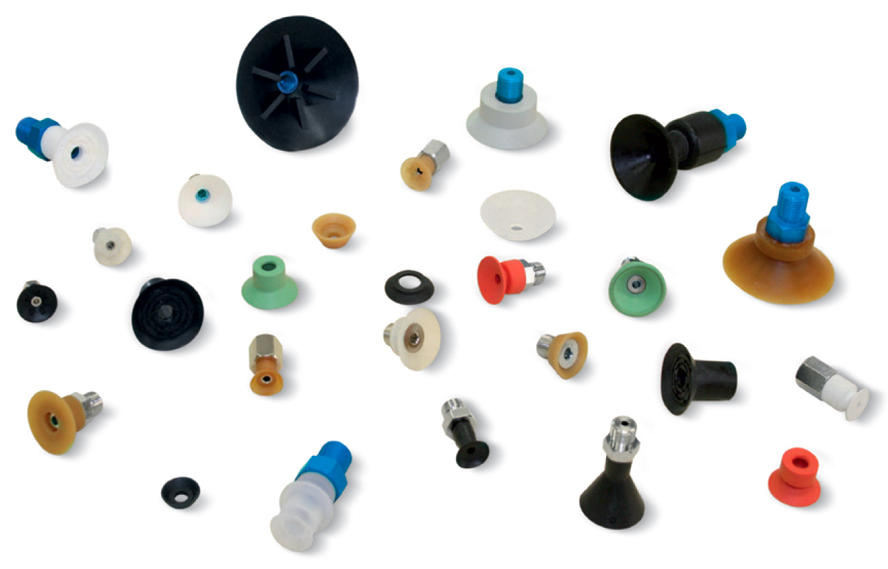
In addition, vacuum cups are the ideal solution for handling chips and other computer components as they do not damage surfaces and do not leave unwanted stains.
Find out more about Vuototecnica’s solutions for the IT sector at www.vuototecnica.net.


